電路顯示LTC1627�����,雙鋰離子至3.3V / 0.5A降壓穩(wěn)壓器
2020-08-21 08:16:56
Switcher 2LT8640S/LT8643S是42 V�����、6 A連續(xù)電流/7 A峰值電流單片式降壓型穩(wěn)壓器�����,采用第二代Silent Switcher? 2架構(gòu)�����。Silent Switcher穩(wěn)壓器通過
2018-10-19 10:28:33
/ LT8608是易于使用的單片降壓型穩(wěn)壓器集成了功率MOSFET和內(nèi)置的補(bǔ)償�����。它們針對具有寬輸入電壓范圍和低EMI噪聲要求的應(yīng)用進(jìn)行了優(yōu)化�����。其2.5μA靜態(tài)電流和突發(fā)模式操作選項(xiàng)使其成為電池供電降壓
2019-03-09 11:42:56
LT8609�����,LT8609 A�����,LT8609 B和LT8609小號是同步單片降壓調(diào)節(jié)器中配有寬3V至42V的輸入范圍�����。該器件系列針對要求低EMI�����,高效率和小尺寸解決方案的應(yīng)用進(jìn)行了優(yōu)化 - 適用于要求苛刻的汽車�����,工業(yè)�����,計(jì)算和通信應(yīng)用�����。該系列中的所有穩(wěn)壓器具有相同的2A連續(xù)�����,3A瞬態(tài)(
2018-08-17 22:05:12
LT8609�����,LT8609 A,LT8609 B和LT8609小號是同步單片降壓調(diào)節(jié)器中配有寬3V至42V的輸入范圍�����。該器件系列針對要求低EMI�����,高效率和小尺寸解決方案的應(yīng)用進(jìn)行了優(yōu)化�����,適用于要求苛刻的汽車�����,工業(yè)�����,計(jì)算和通信應(yīng)用�����。該系列中的所有穩(wěn)壓器具有相同的2A連續(xù)�����,3A瞬態(tài)(
2018-09-13 14:31:04
DN573:42V�����,2A / 3A峰值同步降壓型穩(wěn)壓器�����,具有2.5μA靜態(tài)電流和超低EMI輻射
2019-04-28 07:14:25
LTC4080�����,全功能鋰離子充電器�����,具有熱管理和高效降壓穩(wěn)壓器�����,采用緊湊的單IC解決方案�����。 LTC4080是一款全功能�����,單節(jié)4.2V鋰離子電池充電器�����,集成同步降壓DC / DC轉(zhuǎn)換器�����,主要用于手持式應(yīng)用
2020-06-02 11:53:35
的開關(guān)性能�����,需要高達(dá)3A的雙輸出應(yīng)用提供占板面積非常緊湊的解決方案�����。 日前�����,凌力爾特公司(以下簡稱“Linear”)宣布推出兩款高效率�����、4MHz同步降壓型穩(wěn)壓器“LTC
2018-09-28 16:24:46
�����。所有版本都有現(xiàn)貨供應(yīng)�����。如需更多信息�����,請登錄 www.linear.com.cn/product/LTC3649 �����?����! ≌掌f明:60V�����、4A 單片同步降壓型穩(wěn)壓器可提供 95% 效率和軌至軌輸出
2018-11-30 17:19:55
提高了其熱性能 LTC3255或者以2:1或1:1的轉(zhuǎn)換比作為通用降壓型充電泵工作�����,或者作為電流倍增并聯(lián)穩(wěn)壓器工作�����?����! ?)常模式時,轉(zhuǎn)換比是基于VIN�����、VOUT和負(fù)載情況選擇�����,轉(zhuǎn)換模式之間的切換
2018-09-26 15:43:26
具2.5 μA靜態(tài)電流和超低EMI的 42 V單片式同步降壓型穩(wěn)壓器
2021-02-01 07:38:05
LTM4693超薄低VIN�����,2A降壓升壓μ模塊穩(wěn)壓器LTM4693是一款超薄型�����、高效率的 2A 降壓-升壓 μModule? DC/DC 轉(zhuǎn)換器�����,專為應(yīng)對復(fù)雜電源需求而設(shè)計(jì)�����。其獨(dú)特之處在于能夠在
2025-05-13 09:45:09
LTM4707 μModule穩(wěn)壓器LINEAR
LTM4707是一款由LINEAR提供的 16A 降壓 Silent Switcher 3 μModule穩(wěn)壓器�����,具有超低噪聲和低電磁干擾(EMI
2025-02-27 09:41:35
引言 具有電流和溫度監(jiān)視功能的 LTC3626 同步降壓型穩(wěn)壓器是凌力爾特的單片式穩(wěn)壓器 SWITCHER+ 產(chǎn)品線的首款器件�����。該器件是一款高效率�����、單片式同步降壓型開關(guān)穩(wěn)壓器�����,其能夠采用
2018-09-26 16:21:07
同步降壓穩(wěn)壓器LTC3614資料下載內(nèi)容主要介紹了:LTC3614引腳功能LTC3614內(nèi)部方框圖LTC3614典型應(yīng)用電路LTC3614極限參數(shù)
2021-03-29 07:18:50
同步降壓型穩(wěn)壓器LTC3543資料下載內(nèi)容主要介紹了:LTC3543功能和特性LTC3543引腳功能LTC3543內(nèi)部方框圖LTC3543典型應(yīng)用電路
2021-03-26 08:02:29
同步降壓型穩(wěn)壓器LTC3618資料下載內(nèi)容主要介紹了: LTC3618功能和特性 LTC3618引腳功能 LTC3618典型應(yīng)用電路 LTC3618典型應(yīng)用電路
2021-03-30 07:36:49
如何采用BGA封裝的低EMI μModule穩(wěn)壓器簡化設(shè)計(jì)�����?
2021-06-17 07:49:10
在設(shè)計(jì)有源器件時,有時會出現(xiàn)線性穩(wěn)壓器或開關(guān)穩(wěn)壓器是否更適合設(shè)計(jì)的問題�����。了解兩者之間的差異可以幫助您為您的應(yīng)用程序做出正確的選擇�����。線性穩(wěn)壓器開關(guān)穩(wěn)壓器設(shè)計(jì)靈活性巴克降壓(顯示)�����,升壓�����,降壓 - 升壓
2018-10-24 09:45:34
V至+35 V輸入提供高達(dá)4 A輸出電流的–5 V電源�����。結(jié)論LTM8003是一款采用Silent Switcher架構(gòu)的寬輸入和輸出范圍�����、低噪聲�����、3.5 A降壓型μModule穩(wěn)壓器�����。依靠3.4 V
2018-10-30 11:33:59
應(yīng)用�����。TPS23753APW 包含基于 PoE 的器件和 PWM 控制器功能主要特色對 PoE 電源和適配器電源具有高效率(高達(dá) 90% 以上)輸出為 5V/2.3A具有同步整流器的隔離式反激小尺寸解決方案將 TPS23753APW 與 PoE 接口 PD 和 PWM 控制器結(jié)合使用此電路設(shè)計(jì)經(jīng)過全面功能測試�����,推薦用于新設(shè)計(jì)
2018-08-03 08:38:04
應(yīng)用�����。TPS23753APW 包含基于 PoE 的器件和 PWM 控制器功能特性對 PoE 電源和適配器電源具有高效率(高達(dá) 90% 以上)輸出為 5V/2.3A具有同步整流器的隔離式反激小尺寸解決方案將 TPS23753APW 與 PoE 接口 PD 和 PWM 控制器結(jié)合使用此電路設(shè)計(jì)經(jīng)過全面功能測試�����,推薦用于新設(shè)計(jì)
2022-09-21 06:42:37
�����。20用于SoC的20 V輸入解決方案該LTC7150S提出了用于工業(yè)和汽車電源,高性能的吧�����。它具有高效率�����,小外形和低EMI�����。集成的高性能MOSFET和熱管理功能可在高達(dá)20V的輸入電壓下實(shí)現(xiàn)高達(dá)20A
2018-09-13 14:28:48
開關(guān)或LDO穩(wěn)壓器�����。圖1降壓轉(zhuǎn)換器的原理圖和效率:20 A時12 V IN至1.2 V OUT靜音切換器2具有出色的EMI性能在高電流下通過EMI規(guī)則通常涉及復(fù)雜的設(shè)計(jì)和測試挑戰(zhàn)�����,包括在解決方案尺寸
2019-03-09 11:46:55
采用+5 V至+35 V輸入提供高達(dá)4 A輸出電流的–5 V電源�����。結(jié)論LTM8003是一款采用Silent Switcher架構(gòu)的寬輸入和輸出范圍�����、低噪聲�����、3.5 A降壓型μModule穩(wěn)壓器�����。依靠
2018-10-26 11:48:07
LTC3623IUDD 12V至10A�����,2相單輸出穩(wěn)壓器的典型應(yīng)用電路�����。 LTC3623是一款高效率�����,單片式同步降壓穩(wěn)壓器�����,其輸出電壓可通過單個外部電阻進(jìn)行編程
2020-04-21 10:02:39
LTC7103-1是一款高效率、單芯片同步降壓DC/DC轉(zhuǎn)換器�����,采用恒頻平均電流模式控制架構(gòu)�����。它在4.4V至105V的輸入電壓范圍內(nèi)工作�����,并提供1V至VIN的可調(diào)穩(wěn)壓輸出電壓�����,同時提供高達(dá)2.3A
2023-05-23 16:09:17
LTC?7103 是一款高效率�����、單片式同步降壓型 DC/DC 轉(zhuǎn)換器�����,其采用一種恒定頻率、平均電流模式控制架構(gòu)�����。該器件在 4.4V 至 105V 的輸入電源范圍內(nèi)工作�����,并在輸送高達(dá) 2.3A 輸出
2023-05-24 09:53:14
Linear LT3509雙路36V降壓開關(guān)穩(wěn)壓器應(yīng)用方案
?Linear 公司的LT3509是雙路3.6V-36V電流模式降壓開關(guān)穩(wěn)壓器,每路的內(nèi)部開關(guān)能提供700mA的輸出電流,集成了過壓關(guān)閉和逐個周
2009-11-09 16:30:11 1709
1709 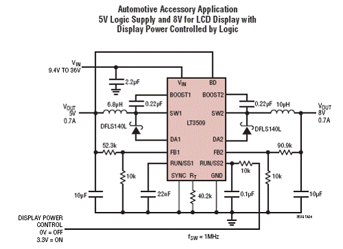
Linear推出1.2A�����、55V 降壓型開關(guān)穩(wěn)壓器
凌力爾特公司 (Linear Technology Corporation) 推出 1.2A�����、55V 降壓型開關(guān)穩(wěn)壓器 LT3991�����,該器件具有一個集成的升壓二極管�����。其突發(fā)模式 (Burst
2009-11-25 09:13:22646 Linear推出高效率4MHz同步2.5A降壓型穩(wěn)壓器
凌力爾特公司 (Linear Technology Corporation) 推出高效率�����、4MHz 同步降壓型穩(wěn)壓器 LTC3604�����,該器件采用一種獨(dú)特的恒定頻率/受控的
2010-02-05 08:56:181177 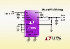
Linear推出同步雙輸出降壓型穩(wěn)壓器
凌力爾特公司 (Linear Technology Corporation) 推出高效率�����、4MHz 同步雙輸出降壓型穩(wěn)壓器 LTC3633�����,該器件采用一種獨(dú)特的恒定頻率/受
2010-02-21 08:34:021353 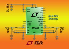
Linear推出同步雙輸出降壓型穩(wěn)壓器LTC3633
凌力爾特公司 (Linear Technology Corporation) 推出高效率�����、4MHz 同步雙輸出降壓型穩(wěn)壓器 LTC3633�����,該器件采用一種獨(dú)特的恒定頻率/受控
2010-02-23 10:08:571710 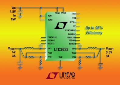
60V輸入雙路輸出同步降壓型穩(wěn)壓器LTC3616(Linear)
Linear凌力爾特公司推出高效率、4MHz 同步降壓型穩(wěn)壓器 LTC3616�����,該器件采用恒定頻
2010-03-20 18:04:291768 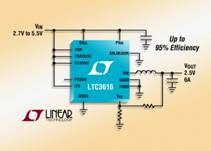
高效率同步降壓型穩(wěn)壓器LTC3614(Linear)
LTC3614器件采用恒定頻率�����、電流模式架構(gòu)�����,能夠?qū)崿F(xiàn)高達(dá) 4MHz 的開關(guān)頻率�����。低電阻內(nèi)部開關(guān)
2010-04-17 10:21:551211 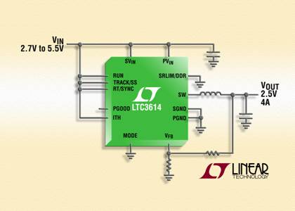
Linear推出高效率�����,4MHz同步降壓型穩(wěn)壓器LTC3615
凌力爾特公司(Linear Technology Corporation) 推出高效率�����,4MHz同步降壓型穩(wěn)壓器 L
2010-05-05 09:48:16849 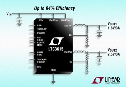
開關(guān)穩(wěn)壓器的EMI解決方案 大多數(shù)開關(guān)穩(wěn)壓器的工作頻率都可利用一個外部時鐘來控制�����,而這個外部時鐘又決定了所產(chǎn)生EMI的基本頻率�����。利用這個特點(diǎn)可以將EMI設(shè)定在一個敏感頻段之外�����,而且�����,當(dāng)同時運(yùn)作多個開關(guān)穩(wěn)壓器時�����,這是一個極為有用的特點(diǎn)�����。當(dāng)時鐘頻率彼此
2011-01-25 16:17:53 49
49 是一款 105V�����、2.3A�����、同步降壓型穩(wěn)壓器�����,其在小型 5mm x 6mm QFN 封裝中納入了一種專有架構(gòu)以實(shí)現(xiàn)超低的 EMI/EMC 發(fā)射�����,并未犧牲效率�����。LTC7103 在 4.4V 至 105V
2018-06-04 13:46:005236 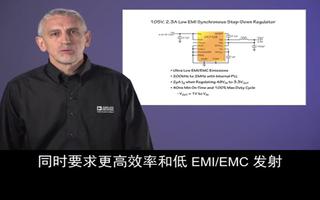
LTC7103 采用一種獨(dú)特的平均電流模式架構(gòu)�����,這在無需使用外部檢測電阻器的情況下實(shí)現(xiàn)了快速和準(zhǔn)確的輸出電流設(shè)置和監(jiān)視�����。8 個引腳可選的固定輸出電壓和任選的內(nèi)部環(huán)路補(bǔ)償可節(jié)省電路板空間和降低靜態(tài)電流�����,同時使得 LTC7103 極為簡單易用�����。
2018-06-28 09:12:004462 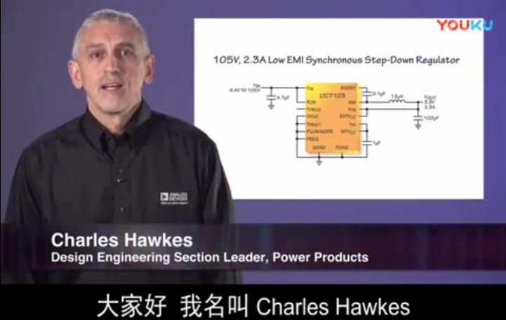
電子發(fā)燒友網(wǎng)為你提供ADI(ti)LTC7103相關(guān)產(chǎn)品參數(shù)、數(shù)據(jù)手冊�����,更有LTC7103的引腳圖�����、接線圖�����、封裝手冊�����、中文資料�����、英文資料�����,LTC7103真值表�����,LTC7103管腳等資料�����,希望可以幫助到廣大的電子工程師們�����。
2019-02-22 14:30:34
105V�����,2.3A低EMI同步降壓穩(wěn)壓器_zh
2019-08-28 06:05:002901 LTC7103: 105V, 2.3A Low EMI Synchronous Step-Down Regulator Data Sheet
2021-01-28 12:44:200 LTC7103 Demo Circuit - High Efficiency, Low EMI Step-Down Regulator (5-100V to 5V @ 2.3A)
2021-02-04 14:48:271 開關(guān)穩(wěn)壓器的 EMI 解決方案
2021-03-21 13:22:043 LT8609S演示電路-2 MHz低EMI高壓同步降壓穩(wěn)壓器(5.5-42V至5V@2A)
2021-04-09 11:47:463 LTC3603演示電路-2.5A�����、15V單片同步降壓穩(wěn)壓器(4-15V至1.8V@2.5A)
2021-04-09 19:15:207 LTC3602演示電路-2.5A�����,10V�����,單片同步降壓穩(wěn)壓器(4.5-10V至2.5V@2.5A)
2021-04-09 19:17:517 LTC3564演示電路-3.3V至1.8V@1.25A單片同步降壓穩(wěn)壓器
2021-04-10 09:10:110 LTC3605演示電路-15V�����、5A�����、4 MHz�����、同步降壓穩(wěn)壓器(12V至1.8V@5A)
2021-04-10 13:46:561 LTC3601演示電路-1.5A�����,15V同步降壓穩(wěn)壓器(12V至1.2V@1.5A)
2021-04-10 13:49:509 LTC3412A演示電路-3A�����、4 MHz、單片同步降壓穩(wěn)壓器(3.3V至1.8V@3A)
2021-04-13 16:34:4910 LTC3605:15V�����,5A同步降壓穩(wěn)壓器數(shù)據(jù)表
2021-04-14 15:24:524 LTC3601:1.5A�����、15V單片同步降壓穩(wěn)壓器數(shù)據(jù)表
2021-04-17 14:32:1310 LTC3604:2.5A�����、15V單片同步降壓穩(wěn)壓器數(shù)據(jù)表
2021-04-25 17:35:557 LTC3633:雙通道3A�����、15V單片同步降壓穩(wěn)壓器數(shù)據(jù)表
2021-04-25 20:24:311 LTC3637:76V�����,1A降壓穩(wěn)壓器數(shù)據(jù)表
2021-04-27 19:36:464 電子發(fā)燒友網(wǎng)為你提供42 V、6 A(峰值7 A)�����、超低EMI輻射�����、 高效率降壓型穩(wěn)壓器資料下載的電子資料下載�����,更有其他相關(guān)的電路圖�����、源代碼�����、課件教程�����、中文資料、英文資料�����、參考設(shè)計(jì)�����、用戶指南�����、解決方案等資料�����,希望可以幫助到廣大的電子工程師們�����。
2021-04-28 08:51:2013 LTC3603:2.5A�����、15V單片同步降壓穩(wěn)壓器數(shù)據(jù)表
2021-04-29 12:55:227 DN48-無設(shè)計(jì)開關(guān)穩(wěn)壓器5V�����,5A降壓(降壓)穩(wěn)壓器
2021-05-08 21:31:004 LTC3633A-2/LTC3633A-3:雙通道3A�����,20V單片同步降壓穩(wěn)壓器數(shù)據(jù)表
2021-05-10 15:03:213 LTC3602:2.5A�����、10V單片同步降壓穩(wěn)壓器數(shù)據(jù)表
2021-05-11 16:45:210 LT7101:105V�����、1A快速電流編程低EMI同步降壓穩(wěn)壓器
2021-05-13 18:04:451 LTC3605A:20V�����,5A同步降壓穩(wěn)壓器數(shù)據(jù)表
2021-05-15 12:24:505 LTC3604項(xiàng)目-2.5A,15V單片降壓穩(wěn)壓器(4.5-15V至1.2V@2.5A)
2021-05-28 19:55:457 LTC3602項(xiàng)目-2.5A�����,10V�����,單片降壓穩(wěn)壓器(4.5-10V至2.5V@2.5A)
2021-05-28 20:13:156 LT8606演示電路-2 MHz低EMI高壓同步降壓穩(wěn)壓器(5.5-42V至5V@350 MA)
2021-05-29 12:33:010 LTC3411A項(xiàng)目-1.25A、4 MHz�����、單片降壓穩(wěn)壓器(2.6-5.5V至1.8V@1.3a)
2021-05-30 09:54:412 LTC3646項(xiàng)目-1A�����,40V單片降壓穩(wěn)壓器(4.5-40V至3.3V@1A)
2021-05-30 12:32:301 LT8609S項(xiàng)目-2 MHz低EMI高壓同步降壓穩(wěn)壓器(5.5-42V至5V@2A)
2021-05-30 17:03:123 LT8607項(xiàng)目-2 MHz低EMI高壓同步降壓穩(wěn)壓器(5.5-42V至5V@750 mA)
2021-05-30 17:09:072 LT8606項(xiàng)目-2 MHz低EMI高壓同步降壓穩(wěn)壓器(5.5-42V至5V@350 MA)
2021-05-30 17:13:326 LTC3601項(xiàng)目-1.5A,15V單片降壓穩(wěn)壓器(4.5-15V至1.2V@1.5A)
2021-05-30 18:15:548 LTC3605項(xiàng)目-15V、5A單片降壓穩(wěn)壓器(5-14V至3.3V@5A)
2021-05-30 18:27:582 LTC3604項(xiàng)目-2.5A,15V單片降壓穩(wěn)壓器(4.5-15V至1.2V@2.5A)
2021-05-30 18:34:066 LTC3601項(xiàng)目-1.5A�����,15V單片降壓穩(wěn)壓器(4.5-15V至1.8V@1.5A)
2021-05-30 18:41:3810 LTC3605A項(xiàng)目-5A�����,20V單片降壓穩(wěn)壓器(4-20V至2.5V@5A)
2021-05-30 18:47:088 LT8608演示電路-2 MHz低EMI高壓同步降壓穩(wěn)壓器(5.5-42V至5V@1.5A)
2021-05-31 09:42:239 LTC3603項(xiàng)目-2.5A,15V單片降壓穩(wěn)壓器(4.5-15V至3.3V@2.5A)
2021-05-31 11:40:280 LTC3417項(xiàng)目-雙4 MHz降壓穩(wěn)壓器(3-5V至1.8V@1.5A和2.5V@1A)
2021-05-31 12:01:021 LTC3633項(xiàng)目-雙3A單片降壓穩(wěn)壓器(3.6-15V至1.5V和2.5V@3A)
2021-05-31 12:49:142 LTC3412A項(xiàng)目-3A�����,4 MHz�����,單片降壓穩(wěn)壓器(2.3-5.5V至1.8V@3A)
2021-05-31 15:17:201 LTC3603項(xiàng)目-2.5A,15V單片降壓穩(wěn)壓器(4.5-15V至3.3V@2.5A)
2021-05-31 15:32:091 LTM8003-3.3演示電路-低EMI降壓模塊穩(wěn)壓器(6-40V至3.3V@3.5A)
2021-05-31 19:07:052 LTM8003演示電路-低EMI降壓模塊穩(wěn)壓器(6-40V至5V@3.5A)
2021-05-31 19:12:200 LTC7149演示電路-反相降壓穩(wěn)壓器(3.4-55V至-5V@2.5A)
2021-06-01 10:35:551 LTC3649演示電路-帶電纜降壓補(bǔ)償?shù)母邏簡握{(diào)同步降壓穩(wěn)壓器(4-60V至5V@4A)
2021-06-01 12:53:032 LTC7103演示電路-高效率、低EMI降壓穩(wěn)壓器(5-100V至5V@2.3A)
2021-06-01 19:30:274 LT8607演示電路-2 MHz低EMI高壓同步降壓穩(wěn)壓器(5.5-42V至5V@750 mA)
2021-06-02 11:57:000 LT8609S演示電路-2 MHz低EMI高壓同步降壓穩(wěn)壓器(5.5-42V至5V@2A)
2021-06-02 14:08:061 LT8609B演示電路-2 MHz低EMI高壓同步降壓穩(wěn)壓器(5.5-42V至5V@2A)
2021-06-02 16:00:435 LTC3622演示電路-雙單片同步降壓穩(wěn)壓器(5-17V至3.3V@1A和5V@1A)
2021-06-04 21:05:5614 LTC3637 76V�����,1A降壓穩(wěn)壓器數(shù)據(jù)表
2021-06-06 19:57:2510 LTM4630演示電路-高效6相105a降壓穩(wěn)壓器(4.5-15V至1V@105a)
2021-06-07 13:26:568 LTC3633A-2演示電路-雙單片同步降壓穩(wěn)壓器(3.6-20V至1.8V3.3V@3A)
2021-06-08 21:03:342 LTC3564演示電路-3.3V至1.8V@1.25A單片同步降壓穩(wěn)壓器
2021-06-09 16:23:21100 LTC3603演示電路-2.5A、15V單片同步降壓穩(wěn)壓器(4-15V至1.8V@2.5A)
2021-06-09 16:31:121 LTC3602演示電路-2.5A,10V�����,單片同步降壓穩(wěn)壓器(4.5-10V至2.5V@2.5A)
2021-06-09 16:36:565 LTC3605演示電路-15V�����、5A�����、4 MHz�����、同步降壓穩(wěn)壓器(12V至1.8V@5A)
2021-06-11 15:25:543 LTC3601演示電路-1.5A�����,15V同步降壓穩(wěn)壓器(12V至1.2V@1.5A)
2021-06-11 15:27:530 LTC3412A演示電路-3A、4 MHz�����、單片同步降壓穩(wěn)壓器(3.3V至1.8V@3A)
2021-06-16 19:35:217
 電子發(fā)燒友App


![[原創(chuàng)] Linear LTC7103 105V 2.3A低EMI降壓穩(wěn)壓器解決方案](/uploads/allimg/180206/0941213446_0.png)
![[原創(chuàng)] Linear LTC7103 105V 2.3A低EMI降壓穩(wěn)壓器解決方案](/uploads/allimg/180206/09415032D_0.png)
![[原創(chuàng)] Linear LTC7103 105V 2.3A低EMI降壓穩(wěn)壓器解決方案](/uploads/allimg/180206/0942021R8_0.png)
![[原創(chuàng)] Linear LTC7103 105V 2.3A低EMI降壓穩(wěn)壓器解決方案](/uploads/allimg/180206/094221a01_0.png)
![[原創(chuàng)] Linear LTC7103 105V 2.3A低EMI降壓穩(wěn)壓器解決方案](/uploads/allimg/180206/0942501460_0.png)
![[原創(chuàng)] Linear LTC7103 105V 2.3A低EMI降壓穩(wěn)壓器解決方案](/uploads/allimg/180206/0943012138_0.png)
![[原創(chuàng)] Linear LTC7103 105V 2.3A低EMI降壓穩(wěn)壓器解決方案](/uploads/allimg/180206/0943214c2_0.png)
![[原創(chuàng)] Linear LTC7103 105V 2.3A低EMI降壓穩(wěn)壓器解決方案](/uploads/allimg/180206/0943515012_0.png)
![[原創(chuàng)] Linear LTC7103 105V 2.3A低EMI降壓穩(wěn)壓器解決方案](/uploads/allimg/180206/09440110G_0.png)
![[原創(chuàng)] Linear LTC7103 105V 2.3A低EMI降壓穩(wěn)壓器解決方案](/uploads/allimg/180206/0944213S0_0.png)
![[原創(chuàng)] Linear LTC7103 105V 2.3A低EMI降壓穩(wěn)壓器解決方案](/uploads/allimg/180206/0945011407_0.png)


 工商網(wǎng)監(jiān)
評論